|
|
|
|
|
|
Research Interests
|
|
|
A particularly interesting aspect of our research in the S2IS lab lies in the combination of expertise from the areas of integrated circuits, systems and sensors design as well as signal/image processing algorithms and their VLSI implementation. Our research can be best described as being in the crossroads between algorithmic solutions and hardware friendly VLSI architecture for sensors applications (vision sensors as well as gas sensors and olfactory systems). The aim behind implementing such algorithmic solutions in CMOS VLSI technologies is to be able to build smart Microsystems in which sensing and processing are integrated as closely as possible hence achieving low cost and low power.
| |
| back top | |
|
|
|
Research Contribution
|
|
|
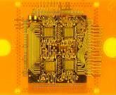
S2IS has made some contributions in the design of vision and olfactory systems with integrated sensing devices as well as novel signal processing architecture integrated either monolithically or using advanced packaging technologies. The group's contributions are mainly related to new VLSI systems offering new technological solutions in which both the sensors and the associated electronics are integrated together enabling low cost, low power and highly efficient on-chip processing. The specific applications in which we started receiving international recognition are in time-domain CMOS image sensors as well as new algorithmic and VLSI architectural solutions for both vision and electronic nose Microsystems. Recently we have successfully implemented low power smart image sensors integrating on-chip image processing operations such histogram equalization and image compression. Our application are not limited to vision sensors but olfaction and gas sensors application mainly targeting gas sensing and gas identification. To this aim, we recently integrated an array of gas sensors and its CMOS pre-processing circuitry. We have also investigated various pattern recognition and gas identification algorithms and succeeded in implementing a novel gas identification system based on Gaussian Mixture Models and committee machine processing.
| |
| back top | |
|
|
|
Key Research areas/projects
|
|
|
Our research interest lies in circuit and system level design of signal/image processing algorithms for sensors and microsystems applications. We are mainly interested in developing new circuits and systems for smart sensors and microsystems. Our team has made some contributions in a number of research project namely:
| |
|
A. Ultra-low power and Energy Harvesting Research
Energy Harvesting CMOS Image Sensors
Due to the recent advancement in wireless communication technologies, new applications (including building, transport, environmental, healthcare etc.) involving various kinds of monitoring have emerged. One of the major advantages in wireless sensing platforms is their ability to provide improved accuracy and density of measurements through the use of large number of sensor nodes. Nonetheless, the conventional battery supplied architecture falls short in these kinds of applications as all the above mentioned advantages will be compromised with frequent energy replenishment, and significant increase in maintenance cost is expected. In that case, scavenging environmental energy (e.g. light, wind, heat, vibrations etc.) for system use becomes beneficial as energy can be readily available from the deployed environment. Instead of incorporating dedicated energy harvesters into these sensing nodes, energy can be harvested using sensors themselves. The reason is that sensors, like energy harvesters, also convert environmental energy into electrical forms. The harvested energy can be significant if array sensors (e.g. image sensors) are reconfigured as energy harvesters. Based on the above insight, I proposed to develop CMOS image sensor that can be reconfigured into energy harvesters during their idle period so that extra energy can be first stored and released for system use later. The following summarizes the important contributions I have made.
i). Asynchronous Pixel for an Energy Harvesting CMOS Image Sensor: I am the pioneering inventor of asynchronous pixel design equipped with an efficient avalanche energy generation (AEG) scheme. The key idea is to lower the sensor array power consumption by enabling only active pixels to be read-out after which they enter into the power generation mode to harvest energy for other active pixels. A very interesting feature about this approach is that during a frame capture, critical energy is mainly required during startup. Once a group of pixels have been readout, the available energy will rise and more array activity will contribute to the generation of more energy, hence creating an avalanche effect. Unlike prior art that requires the introduction of extra energy harvesting elements, this scheme is self-sufficient as the sensor array is also the energy harvester. I have also introduced the theoretical model for both energy generation and power consumption for the sensor array. The performance of the first prototype is also characterized experimentally, verifying the feasibility of this scheme.
ii). Reconfigurable Resolution CMOS Image Sensor with Energy Harvesting Capabilities: In this work, we extend on the previous scheme by incorporating reconfigurable pixels for both sensing and energy harvesting in the sensor array scale. One of the major challenges for realizing a self-powered CMOS image sensor is the unmatched power generation/power consumption property, which can be in a ratio of several decades. In order to solve this problem, we introduced two novel features, namely reconfigurable resolution readout and two-level quantization scheme, into the image sensor architecture design to further lower the system power consumption. A CMOS image sensor array is fully characterized, demonstrating both the image sensing and the energy harvesting capability. An estimated operating cycle of approximately 0.2% can be achieved if the harvested energy is to compensate for the consumed energy in this prototype.
iii). High Voltage Generation with Stacked Photodiodes in Standard CMOS Process: One of the major hurdles in implementing self-powered single-chip systems using integrated energy harvesters is photodiodes fabricated in standard CMOS process can only generate an output voltage of roughly 0.3~0.4V (depending on the illumination level). This voltage is in general too low to be useful in integrated circuits. As the devices in standard CMOS process are substrate tied together, stacking of photodiodes to generate high voltage is in general difficult if not impossible. Prior arts solve this problem either by using multi-chip solution (where the substrate of different chips can be separated on PCB level), or by using high-cost silicon-on-insulator (SOI) process. In our research, we demonstrate that stacking of photodiodes is not beneficial due to the existence of parasitic photodiodes, and proposed a systematic method to compensate for this parasitic loss. My proposed method is experimentally verified, and output voltages of 0.84V and 1.3V are successfully generated by two-stage and three-stage photodiode series connections, respectively. A key benefit in my scheme is that it is readily implementable in Bulk-CMOS technology without the requirement of isolated/custom substrate, hence enabling low cost self-powered system-on-chip (Soc) implementations.
| |
|
B. Advanced CMOS Image Sensor Architecture Research
Highly efficient CMOS Image Sensor with NOC reconfigurable processor array
CMOS image sensors have become one of the fastest growing sectors of the CMOS industry, largely due to the explosive growth of its application in mobile and portable consumer products in recent years. We expect this trend to continue as CMOS image sensor technology further proliferates into emerging applications such as sensor networks, biomedical systems, industrial and military products, buildings, security, etc. Unfortunately, with modern silicon technology scaling, when we reduce the pixel sizes to attain higher resolution and faster frame-rate, it is becoming increasingly difficult to attain a satisfactory compromise between power-consumption, bandwidth, image-quality, reliability and cost at both the process and circuit level.
In conventional practices, the imaging pipeline (a cascade of the photo-sensor, the ADC, the memory, the digital processor, and the software algorithms) is considered and designed in separate sub-block entities. The methodology is robust and easy to manage, but it is far from optimal in terms of performance. In our work, we explore a new style of architecture where parts of the image/video processing and compression algorithms are embedded into the mixed-signal domain at the ADC boundary. Combining this and an advanced reconfigurable processor array built on the Network-on-Chip paradigm, our prototype system will demonstrate how we can achieve the best energy per information trade-off by carefully suppressing information redundancy at each stage of the imaging pipeline: from photo-sensors to processed result.
My research group has proposed a novel compressive readout image sensor with several unconventional and interesting characteristics including: negative processing power budget (the sensor will consume less energy when the read-out data is compressed) and digital motion detection in compressed domain. Results indicate that the energy consumption of our design will be at least one order of magnitude lower than previous works, while imaging speed and quality is significantly higher. The second phase of this work will be focused on the design of an advanced reconfigurable processor array suitable for performing image/video processing, segmentation, and object recognition on the data output of the first prototype. Finally this exciting project involves the design of 3D integrated CMOS circuits, where we are attempting to demonstrate the cost and performance advantage of a vertically integrated CMOS camera with stacked optical lens, sensor, memory, and processor dies.
Polarization-based CMOS Image Sensors
Polarization imaging contains valuable information regarding imaged objects' geometrical, physical, chemical, physiological and metabolic properties that is largely uncorrelated with light intensity or color. As the vectorial characterization of the light reflected or emitted by objects in a scene, polarization imaging provides insightful and complementary data on the physical nature of the objects. Polarization imaging reveals much richer information regarding the imaged scene and enables a wide range of machine vision tasks that are more difficult or even infeasible if limited to the use of only intensity and color information. A camera-on-a-chip offers significant advantages in terms of system miniaturization and manufacturing cost. Like the vast majority of commercially available camera systems, CMOS image sensor is essentially designed to image the world in terms of intensity and color. By coating its individual photosensitive pixels with patterned micrometer-scale polarizing elements (also known as micropolarizing devices), the concept of a compact fully-integrated CMOS polarization image sensor, featuring low cost, low power consumption and on-chip real-time polarization image sensing/processing, is enabled.
In my research group, high-resolution micropolarizing devices were designed, fabricated and characterized for CMOS polarization image sensors to extract Stokes polarization parameters, which fully describe all possible polarization states of incident light. Both absorptive-type and reflective-type linear polarizers are explored to develop CMOS-compatible fabrication technologies of micropolarizing devices for the applications with natural passive light source, such as polarization difference imaging (PDI) and partial-linear polarization imaging (PLPI). Proposed implementations greatly improve previously reported fabrication processes by completely removing the need of complex selective etching and dramatically scaling-down the micropolarizing elements' pitch size and thickness with non-contact photoalignment technique, where the thickness is directly related to the signal cross-talk when applied to scenes with large angle of incidence. In addition, our research is further extended to micropolarizing devices for novel circular polarization imaging, which is always discarded in the previously reported implementations with natural passive light source. However, for applications with artificial collimated active light source, circular polarized components cannot be neglected and their extraction can further reveal a lot more information with respect to the imaged objects.
CMOS Image sensors with integrated on-chip image processing
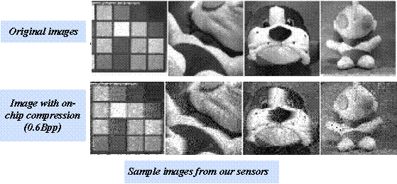
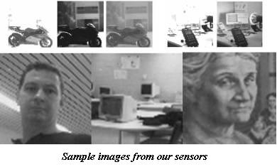
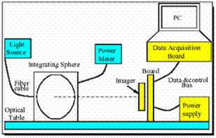 One of the key claimed advantages of CMOS image sensors over its CCD counterpart is the ability of CMOS technology to integrate both image acquisition and on-chip processing. Implementing real-time image processing is however very challenging due to the algorithmic complexity and the very large amount of data to be stored and processed on a real-time basis. For this reason, the claimed advantage of CMOS image sensors has not been fully exploited and only limited simple image processing has been implemented together with image acquisition. In our research, we tackle this issue very profoundly by proposing new time-domain encoding scheme in order to implement complex image processing operations leading to smart vision sensors. We have successfully implemented a low power CMOS image sensor with on-chip image compression. The processing is based on our novel compression algorithm using boundary adaptation quantizer and quadrant tree decomposition technique. In another application, we successfully integrated an image sensor together with histogram equalization processing using time-to-first spike and address event representation.
| |
|
C. Low Power Temperature Sensors for RFID Research
The recent emergence of RFID and wireless sensor network (WSN) applications has given rise to the development of wireless sensing platforms embedded with various sensors. As most everyday systems (including physical, biological, electrical, chemical, mechanical etc.) exhibit some kind of temperature dependency, incorporating temperature sensor inside such wireless platforms is usually required. The major challenge for deployment in such applications is the limited power/energy available in the sensing nodes, as they are mostly randomly deployed in various locations, and hence are usually battery powered or even passively powered (harvest energy from the environment). As a consequence, the power/energy efficiency of the system, instead of sensing range and accuracy requirements, is of utmost importance. The temperature sensor should theoretically consume as little power/energy as possible for improved system lifetime and/or reliability. Hence, a temperature sensor design that consumes nW power so as not to burden the system is desirable. The following summarizes the important contributions I have made with my students.
i). Linear/Subthreshold MOSFET based CMOS temperature sensor design: In my group, we have pioneered the use of MOSFET working in different regions for temperature sensing applications. Prior existing works using MOSFET as temperature sensing element only considers biasing MOSFET in the subthreshold region, without exploiting other possibilities. We have found that instead of using the conventional architecture, MOSFET working in various regions also exhibits reliable linear-to-temperature behavior that can be utilized to achieve ultra-low power temperature sensing. Apart from that, we have proposed the use of differential sensing architecture in time domain readout circuit to compensate for the sensor offset without sacrificing the output SNR, and the use of supply voltage sensing technique to improve the power supply rejection of time domain readout schemes. Using all the optimization techniques described, MOSFET based CMOS temperature sensor consuming as low as 119nW, which is one of the most power efficient CMOS temperature sensor reported to date, is achieved.
ii). Gain compensated CMOS temperature sensor design embedded in passive RFID tag: In this implementation, we have designed a CMOS temperature sensor embedded in a passive RFID tag. All the system level functional/performance tests, including accurate wireless temperature sensing measurement, have been successfully demonstrated. This design exploited the possibility of co-designing with other building blocks inside the tag (specifically the on-chip bandgap reference and the clock generator) to achieve sensor gain compensation so that the effective temperature sensing inaccuracy can be reduced by more than half. A temperature sensing inaccuracy within +/- 0.8 degree Celsius is achieved after low-cost one point calibration, and temperature sensing only requires an additional power of merely 104nW, which is also one of the most efficient to date. This project was a real successful collaboration project with other colleagues within the ECE department. The project was supported by a major ITF grant.
| |
|
D. Electronic Nose Research
Biologically-inspired Electronic Nose Microsystem
The last decade has witnessed an ever growing interest for the development and design of gas/odor identification systems, also known as electronic noses. This interest has been driven by a variety of real-life and newly emerging applications. Examples include the detection of combustible gases to protect workers and infrastructures, air quality and pollution monitoring in cities, agriculture (quality, control, soil contamination, etc.) but also detection of infections, diseases or bacteria. While the domains of electronic nose application keep expanding, the development of a standalone gas identification system suitable for real-life applications still faces a number of challenges. At the sensor level, a lack of selectivity, non-linearity and long-term drift make gas recognition a difficult task and an advanced signal processing stage to process the raw sensors' data is required. In addition, the ability to recognize different gases requires a complex training phase, which is difficult to implement on a dedicated hardware. As a result, electronic nose solutions today are either software-based platforms or expensive bulky devices. To address these limitations, I have proposed to develop low cost yet robust odor identification system, which is described as follows:
Inspired by mammalian olfactory systems, I have designed and fabricated both multi-chips and single-chip prototypes of gas identification systems. These systems are interfaced to an in-house fabricated tin oxide gas sensor array, whose resistances are converted to a unique spike sequence. This sequence is a function of the sensed gas but independent of its concentration. As a result, gas discrimination can be achieved by simply observing the sequence order. Moreover, no prior knowledge of gas concentration is required during the training phase, which further simplifies the calibration procedure. We have demonstrated for the first time a fully integrated electronic nose system integrating a 4X4 tin-oxide gas sensor array together with a biologically inspired spike encoding scheme. This work pioneers the translation of neurophysiological findings into hardware implementation for the processing of gas sensor data featuring a number of advantages such as simple recognition, easy calibration and training. My contribution to biologically-inspired engineering solutions has been recently recognized as evidenced in my recent invitation to serve as an editor for the Frontiers in Neuromorphic Engineering Journal. We have also received a Best paper award from ISCAS 2010 in connection with the work reported in this area.
New technologies for smart gas sensors application
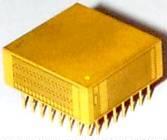
In this research, we have developed a new software/hardware solution that we believe can meet the computational requirement of neural network based classifiers. In the proposed classification algorithm, individual classifiers are decision trees implemented as threshold networks trained independently and combined by a majority vote function. Such a combination has shown improved generalization performance but can require large amounts of memory and computation, a drawback for addressing portable real-time pattern recognition applications. We have addressed this issue by developing a world-first 3D VLSI implementation of bagging ensembles. The 3D chip implements 192 multi-precision neurons operating at a speed of up to 48GCPPS and integrated in a compact chip of (2 X 2 X 0.7) cm3.
| |
|
| |
|
| |
|
| |
| back top | |
|
|
|
Research Grant
|
|
|
1. Integrated Passive UHF RFID Tags and Readers
Source: ITF Grant, ITP/027/07LP, 2007-09
Investigator: Howard Luong and other faculty
2. Self-Powered Self-Timed CMOS image sensor for ultra-low power portable imaging systems
Source: Research Grant Council, Competitive Earmarked Research Grant, 2007-09
Investigator: Amine Bermak (project manager) and C.Y Tsui
3. A Computationally Extensive Biometric AER CMOS Image Sensor
Source: Research Grant Council, Competitive Earmarked Research Grant, 2006-08
Investigator: Amine Bermak
4. CMOS image sensor with integrated face detection processing
Source: Post-doctoral Fellowship Matching Fund, PDF, HKUST,2007
Investigator: Amine Bermak and Farid Flitti
5. BIOSENS (BIO-Inspired SENSing)
Source: INRIA-Hong Kong Joint Research Team, 2006-08
Investigator: Dominique Martinez (Project Manager) and Amine Bermak
6. Integrated Smart Biometric Systems
Source: Emerging High Impact Area, HKUST, 2006-07
Investigator: Amine Bermak (Project Manager) and other faculty
7. Low-Power and High-Throughput Reconfigurable Arithmetic Opera. for FPGA
Source: Germany/Hong Kong RGC Joint Research Grant, 2006-07
Investigator: Amine Bermak and Hans Pfleiderer
8. T-Modulated TO Sensors and Bio-Inspired Processing for EN Applications
Source: France/Hong Kong RGC Joint Research Grant (PROCORE), 2006-07
Investigator: Amine Bermak and Dominique Martinez
9. Robust Pattern Recognition Algorithms for Electronic Nose Applications
Source: Research Grant Council, Competitive Earmarked Research Grant, 2005-07
Investigator: Amine Bermak (Project Manager) and Philip Chan
10. Power Optimization and Management Techniques for FPGA Implementation
Source: British Engineering & Physical Sciences Research Council EPSRC,2005-06
Investigator: Abbes Amira (Project Manager) and Amine Bermak
11. A Smart Vision Sensor with FP ADC and Pulse Sensory Image Processing
Source: Research Grant Council, Competitive Earmarked Research Grant,2004-06
Investigator: Amine Bermak
12. EN Microsystem Based on an Array of Gas Sensors and Advanced PRA
Source: France/Hong Kong RGC Joint Research Grant (PROCORE), 2004-05
Investigator: Amine Bermak and Dominique Martinez
13. Advanced PR Algorithms for Odor Classification and Quantification
Source: Post-doctoral Fellowship Matching Fund, PDF, HKUST, 2004
Investigator: Amine Bermak and S. B.Belhouari
14. Reconfigurable NN VLSI Classifier for Miniaturized Odor Sensing Systems
Source: Direct Allocation Grant, DAG, RGC, 2003-04
Investigator: Amine Bermak
| |
| back top | |
|
|
|