|  | |
|
It takes 6-12 months to go through the process of integrating an idea into a chip. The cycle includes design and simulation, fabrication and finally test and characterization. We have an average of 2 VLSI chips designed per year.
The followings are our selected Chip Gallery:
|
|
|
| |
|
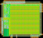
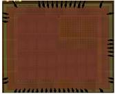
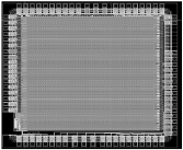
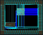
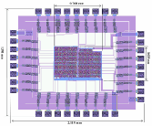
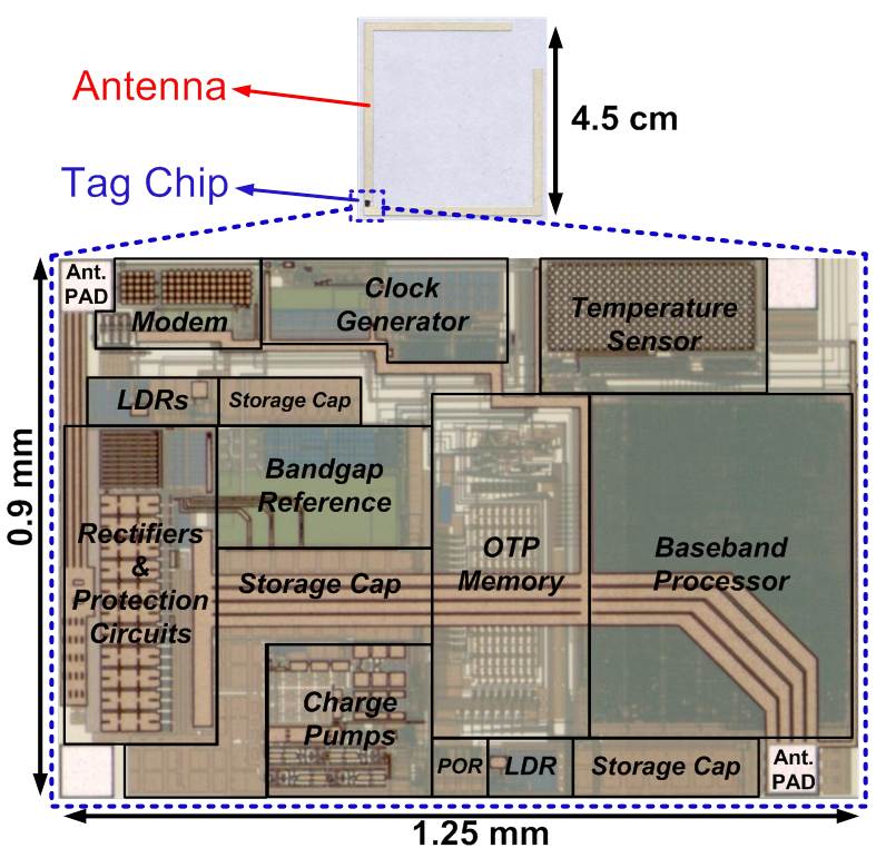 JSSC-Tag
Designer: Dr. M. K. Law, Prof. A. Bermak and colleagues
Date: 2010
This prototype exploits the concept of co-designing of embedded temperature sensor with the system clock and bandgap reference. A sensor gain compensation scheme is utilized so that only one-point calibration is required to reduce cost. The sensor readout consumes only 104-nW and achieves a 3-sigma sensing accuracy of +/- 0.8^oC from -20 to 30^oC. This is one of the lowest power CMOS temperature sensor ever reported in literature.
|
|
|
| |
|
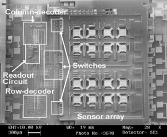
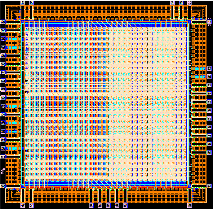
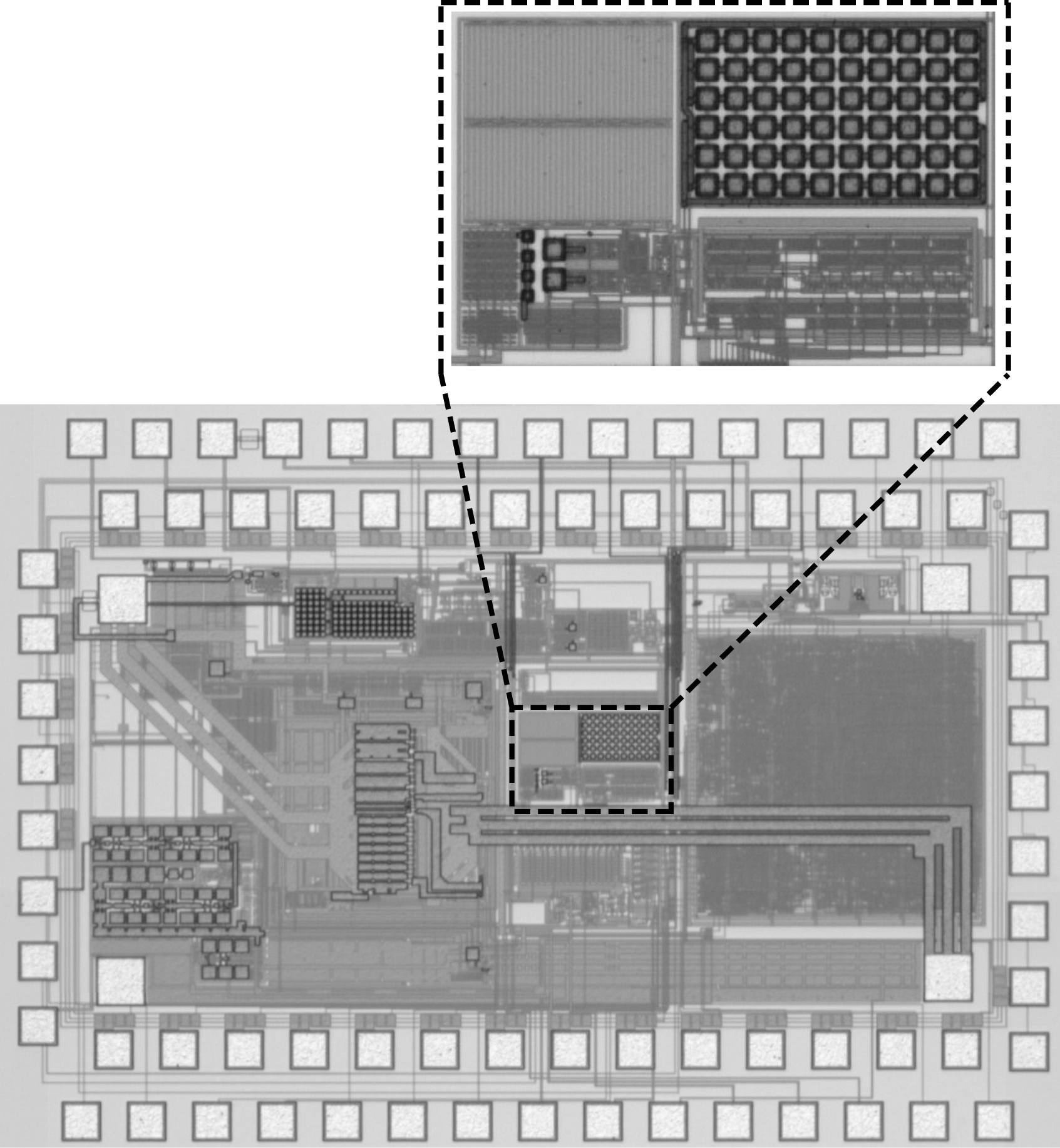 JSSC-Sensor
Designer: Dr. M. K. Law, Prof. A. Bermak and colleagues
Date: 2009
The CMOS temperature sensor is embedded in the RFID tag system. By using a supply voltage of 0.5-V, the sensor consumes only 119-nW while achieving a sensing accuracy of +/-1^oC from -10 to 30^oC, which is suitable for RFID food monitoring application. This is one of the lowest power CMOS temperature sensor ever reported in literature.
|
|
|
| |
|
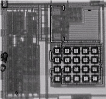
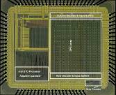
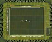
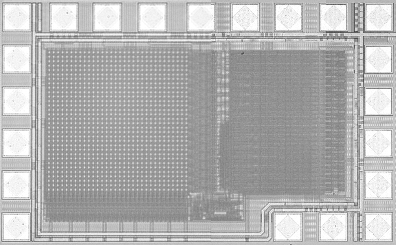 TCASII-EHImager
Designer: Dr. M. K. Law, Prof. A. Bermak and colleagues
Date: 2010
This prototype can perform both image capture and energy harvesting by using the same reconfigurable photodiode sensor array. It is fabricated using the AMS 0.35um standard CMOS process. Power consumption is optimized by using two-level quantization scheme.
|
|
|
| |
|
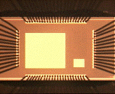
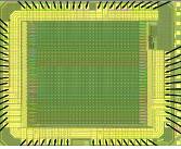
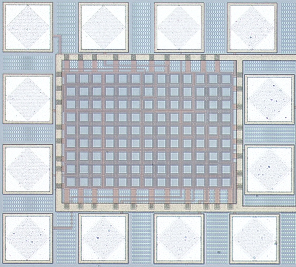 EDL-HVPD
Designer: Dr. M. K. Law, Prof. A. Bermak and colleagues
Date: 2009
This structure verifies the proposed systematic approach for generating a high open-circuit voltage using serially connected integrated photodiodes in AMS 0.35um standard Psub/NWell CMOS process. By compensating the effects of parasitic photodiodes, an open-circuit voltage of 1.34V is realized without using expensive SOI process.
|
|
|
| |
|
 TCASII-LinearTS
Designer: Dr. M. K. Law, Prof. A. Bermak and colleagues
Date: 2009
Fabricated in the TSMC 0.18um CMOS process, this temperature sensor utilizes MOSFET operating in linear region as the sensing element. Together with a differential time-domain readout architecture, a sensing accuracy of +/- 1^oC within 0 to 100^oC can be achieved using only 405-nW from 1-V supply.
|
|
|
| |
|
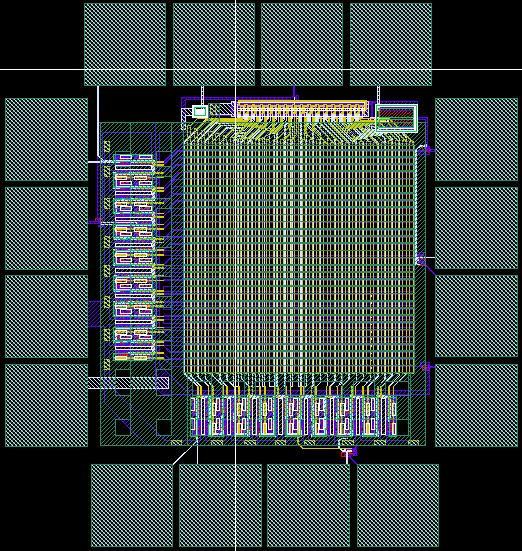 A 4-T CMOS current-mediated imager
Designer: F. Tang and Prof. A. Bermak
Date: 2009
A 4-T CMOS current-mediated imager with in-pixel 2-bit control lines. For each operating cycle, only one pixel is reset while another one pixel is read out.
|
|
|
| |
|
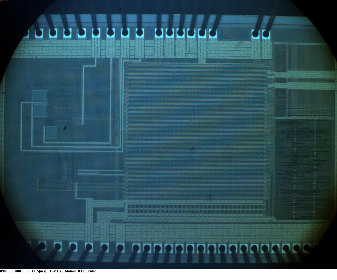 TFS sensor with on chip image compression based on predictive boundary and QTD algorithm
Designer: Dr. S. Chen and Prof. A. Bermak
Date: 2008
TFS sensor with on chip image compression based on predictive boundary adaptation and QTD algorithm. Fabricated in Alcatel 0.35um CMOS technology, 2007. The image data is first scanned following Hilbert scanning strategy. The acquired image is then compressed by a processor which is based on Fast Boundary Adaptation Rule, Differential Pulse Code Modulation and on-line QTD algorithm.
|
|
|
| |
|
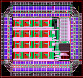 4x4 Log-timing-delay spiking neuron array with the control unit & detection circuits
Designer: Dr. B. Guo and Prof. A. Bermak
Date: 2007
It can perform gas detection and quantification which are realized by processing the spike rank order and the time to the first spike latency, respectively. The advantage of this scheme include its simple structure and computation efficiency, which make it an attractive solution for the integrated electronic nose micro-systems.
|
|
|
| |
|
 64x64 TFS sensor with on chip image compression based on predictive boundary adaptation
Designer: Dr. S. Chen and Prof. A. Bermak
Date: 2007
The Chip is Fabricated in Alcatel 0.35um CMOS technology. The image data is first scanned following Hilbert scanning strategy. The acquired image is then compressed using a predictive Fast Boundary Adaptation Rule using Differential Pulse Code Modulation followed by on-line QTD algorithm.
|
|
|
| |
|
 CMOS Image Sensor with on-chip Image compression processor
Designer: Dr. S. Chen, Y. Wang (Mphil student)
and Prof. A. Bermak
Date: 2006
The Chip integrates a digital pixel sensor with image compression processor based on boundary adaptive quantizer and Quadrant Tree Decomposition processing.
|
|
|
| |
|
 A Monolithically integrated tin oxide 4x4 gas sensor array with on-chip pre-processing
Designer: Dr. B. Guo and Prof. A. Bermak and colleagues at HKUST and Beijing University
Date: 2006
MEMS/CMOS circuit integrating on the same die an array of 4x4 tin-oxide gas sensing devices, read-out and pre-processing circuitries.
|
|
|
| |
|
 Color Image sensor in 0.18um CMOS Process
Designer: X. Zhao (PhD student), A. Bermak
Date: 2006
This prototype integrates test RGB 3D photodetectors with their read-out circuit in 0.18um CMOS process.
|
|
|
| |
|
 Gaussian Mixture Model (GMM) VLSI classifier for Electronic Nose applications
Designer: Dr. M. Shi and Prof. A. Bermak
Date: 2005
The chip Integrates a GMM Classifier featuring a novel pipelining architecture and a linear piecewise approximation of GMM classifier. This is the first GMM chip implementation ever reported.
|
|
|
| |
|
 Arbitrated Time-to-First Spike CMOS imager with histogram equalization
Designer: Dr. S. Chen and Prof. A. Bermak
Date: 2005
The Chip integrates an asynchronous CMOS Image Sensor using TFS encoding and on-chip histogram equalization processing. This is probably the first imager including Histogram Equalization and arbitrated TFS.
|
|
|
| |
|
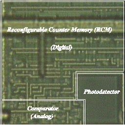 A novel pixel level counter/memory for spiking pixel image senor
Designer: Dr. S. Chen and Prof. A. Bermak
Date: 2004
Test structures integrating a novel memory/counter circuit using dynamic and static memory cell for spiking pixels.
|
|
|
| |
|
 A reconfigurable resolution and conversion time digital CMOS image sensor
Designer: Y.F. Yung (Mphil student) and A. Bermak
Date: 2003
The chip integrates a reconfigurable resolution of 32x32/64x32 and 8-b/4-b conversion modes. Around 16 times frame-rate speed-up is achieved when using 4-b coding resolution. The imager also features reconfigurable spatial resolution dynamic range.
|
|
|
| |
|
 A Time-domain digital pixel sensor with pulse width modulation Scheme
Designer: A. Kitchen (Mphil student) and A. Bermak
Date: 2002
The chip integrates a 64x64 CMOS image sensor with time domain encoding. The chip features a high dynamic range of over 100dB.
|
|
|
| |
|
 A CMOS Image Sensor with Delta-Sigma pixel level ADC
Designer: A. Bermak, and colleagues
Date: 2001
The chip integrates a CMOS image sensor with delta-sigma digital pixel sensor in 0.25um CMOS process. The work laid the foundations for the establishment of a start-up company (IPI) in Perth, Australia.
|
|
|
| |
|
 Vision Chip with image capture and on-chip biologically inspired shunting inhibition processing
Designer: A. Bermak
Date: 2000
The chip integrates a CMOS image sensor together with an on-chip image enhancement and edge detection processor using current mode shunting inhibition biologically inspired processing.
|
|
|
| |
|
 CMOS Image Sensor with logarithmic pixel
Designer: A. Bermak
Date: 1999
The chip integrates a CMOS image sensor with three different architectures of logarithmic pixels together with the associated control circuit and successive approximation 8-bit ADC.
|
|
|
| |
|
 VLSI Correlation Matrix Memory Neural Network
Designer: A. Bermak
Date: 1998
A VLSI implementation of an artificial neural network (ANN) accelerator based on correlation matrix memory (CMM) for classification applications.
|
|
|
| |
|
 A Three dimensional VLSI Classifier for bagging Threshold network ensembles
Designer: A. Bermak
Date: 1999
The first ever 3D chip integrating 192 digital multi-precision processing elements PEs integrating 768 synapses in a module size of 2x2x0.7cm3. The chip was used for pattern recognition applications (gas discrimination and Electronic Nose applications).
|
|
|
| |
|
 Multi-Chip Modules (MCM)
Designer: A. Bermak
Date: 1998
MCM integrating four VLSI chips occupying an area of 2x2cm2. The MCM is used as an intermediate step in a 3D MCM-vertical process. The MCM also includes a temperature sensor enabling to monitor the temperature of the 3D module.
|
|
|
| |
|
 SysNeuro: A Systolic Multi-precision Neural Network Chip
Designer: A. Bermak
Date: 1997
The chip implements a two-dimensional systolic array architecture which could be configured to perform various binary neural network topologies with a programmable precision (for both synaptic weights and input patterns).
|
|
|
| |
|
 A variable precision Baugh-Wooley 4/8/16-b Multiplier for NN applications
Designer: A. Bermak
Date: 1995
Prof.Bermak's first full-custom VLSI chip integrating a reconfigurable 4/8/16 Baugh-Wooley binary/2’s complement multiplier. The design was reported to have the highest integration density as compared to other designs at that time.
|
|
|
| |
|
| |