|
|
|
|
|
 |
Post-Doctoral Research Associate
Email : denischn@gmail.com
Office : Rm3124
|
|
|
|
Research
|
|
|
Thesis Title : Successive-Approximation-Register Analog-to-Digital-Converter for Low-power CMOS Image Sensing and Compression
Supervisor : Prof. Amine Bermak
Key words : Sensor System-on-Chip (SoC), low-power SAR Analog-to-Digital Converter (ADC), CMOS image sensors, Analog-to-Information Converters (AIC), compressive image sensing, error-correction ADC
|
|
|
Selected Publications
|
|
|
Journals
[8] D. G. Chen, M.-K. Law, F. Tang, L. Yong, and A. Bermak, "CMOS Laser Doppler Imaging with Body-Biased Pixel Reset and 16-bit SAR ADC Array," in preparation.
[7] D. G. Chen, F. Tang, M.-K. Law, and A. Bermak, "An 44 fJ/state 9-bit SAR ADC Array with Forward Error Correction and mixed-signal CDS for CMOS Image Sensors in Retinal Prosthesis," in preparation.
[6] F. Tang, D. G. Chen and A. Bermak, "Continuous-Time Sigma-Delta ADC With Implicit Variable Gain Amplifier For CMOS Image Sensor," in preparation.
[5] D. G. Chen, F. Tang, M.-K. Law, and A. Bermak, "A 12 pJ/pixel Analog-to-Information Converter based 816 $\times$ 640 CMOS Image Sensor," IEEE Journal of Solid-State Circuits, major revision.
[4] F. Tang, D. G. Chen, B. Wang, and A. Bermak, "CMOS On-Chip Stable True-Random ID Generation Using Antenna Effect," IEEE Electron Device Letters, accepted.
[3] D. G. Chen, F. Tang, and A. Bermak, "A Low-Power Pilot-DAC Based Column Parallel 8b SAR ADC With Forward Error Correction for CMOS Image Sensors," IEEE Transactions on Circuits and Systems I: Regular Papers, vol.60, no.10, pp.2572,2583, Oct. 2013. 
[2] F. Tang, D. G. Chen, B. Wang, and A. Bermak, "Low-Power CMOS Image Sensor Based on Column-Parallel Single-Slope/SAR Quantization Scheme," IEEE Transactions on Electron Devices, vol.60, no.8, pp.2561,2566, Aug. 2013.
[1] D. G. Chen, D. Matolin, A. Bermak, and C. Posch, "Pulse-Modulation Imaging - Review and Performance Analysis," IEEE Transactions on Biomedical Circuits and Systems, vol.5, no.1, pp.64-82, Feb. 2011.
Conferences
[7] P. J.-H. Lee, D. G. Chen, A. Bermak, and M.-K. Law, "A High Voltage Zero-static Current Voltage Scaling ADC Interface Circuit for Micro-Stimulator," Proceeding of IEEE International Symposium on Circuits and Systems (ISCAS 2014), Melbourne, Australia, June 1-5, 2014.
[6] D. G. Chen, and A. Bermak, "Protecting Water Resources via Smart-Sensing Infrastructure: From Silicon to Systems," Proceeding of Qatar Annual Research Conference, Doha, November 24 - 25, 2013.
[5] D. A. Soysa, O. C. Au, L. Sun, L. Xu, J. Li, and D. G. Chen, "Advanced Independent Cascade Model for YouTube Content Propagation in Facebook," Proceeding of IEEE China Summit and International Conference on Signal and Information Processing (ChinaSIP), 6-10 July 2013, Beijing, China.
[4] D. A. Soysa, D. G. Chen, O. C. Au, and A. Bermak, "Predicting YouTube Content Popularity via Facebook Data: A Network Spread Model for Optimizing Mul- timedia Delivery," Proceeding of IEEE Symposium Series on Computational Intelligence (SSCI), 15-19 Apr. 2013, Singapore.
[3] D. G. Chen, and A. Bermak, "A Low-power Dynamic Comparator with Digital Calibration for Reduced Offset Mismatch," Proceeding of IEEE International Symposium on Circuits and Systems (ISCAS 2012), Seoul, Korea, May 20-23, 2012.
[2] D. G. Chen, A. Bermak, and C. Y. Tsui, "A low-complexity image compression algorithm for Address-Event Representation (AER) PWM image sensors," Proceeding of IEEE International Symposium on Circuits and Systems (ISCAS 2011), pp.2825-2828, Rio de Janeiro, Brazil, May 15-18, 2011.
[1] D. G. Chen and K.W. Eccleston, "Substrate Integrated Waveguide with Corrugated Wall," Proceeding of 2008 Asia-Pacific Microwave Conference, 16-20 Dec. 2008.
|
|
|
Selected Chip Gallery
|
|
|
|
|
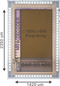
MONAVALE -- Laser Doppler Imaging Sensor
Applications: Flowmetry, Blood Perfusion Monitoring, Biometrics, Air Particular (PM 2.5) Counting
Designer: Dr. D. G. Chen
Date: 2013
Laser Doppler Imaging (LDI) directly images fluid
flow and blood perfusion by observing their velocity induced
Doppler Shift. This chip uses a non-CDS pixel readout scheme along with a
low-noise 16b SAR ADC for high resolution LDI. Measurement
results from the prototype chip in 0.18 um technology show that
the body-biased PMOS-reset pixel readout scheme improves the
LDI flow-rate sensing accuracy by 6.9 dB. The 16b SAR ADC
improves the sensing accuracy by 4.4 dB when compared to 10b
resolution. The ADC circuit occupies 518 um x 84 um and is
suitable for column parallel implementation in low-power CMOS
image sensors. The ADC's Differential Non-Linearity (DNL) is
+3.0/-2.8 LSB and its Integral Non-Linearity (INL) is +24/-17
LSB. The ADC's input referred noise is 110 uVrms making its
ENOB 13.6 bits and its Figure-of-Merit (FoM) 31 fJ/state which
is competitive even against the best published general-purpose
image sensors.
|
| |
|
| |
|
|
|
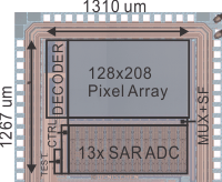
HIGHSTED -- CMOS Image Sensor with Low-power SAR ADC
Applications: Mobile, Security, Retinal Prosthesis, Smart Infrastructure
Designer: Dr. D. G. Chen
Date: 2012
A CMOS Image Sensor with 9b Successive-Approximation-Register (SAR) Anglog-to-Digital Converter (ADC) based on
pilot-Digital-to-Analog Converter (pDAC). The ADC measures
490 um x 7.4 um and is suitable for application in low-power CMOS image sensors
with column parallel ADCs. Measurement results from a prototype chip in 0.18 um technology show
that the ADC's Differential Non-Linearity (DNL) is reduced from 3.5 LSB to 1.2 LSB by the proposed
mixed-signal FEC algorithm, making the effective Figure-of-Merit (FoM) 44 fJ/state. Furthermore, when
combined with the proposed mixed-signal Correlated-Double-Sampling, the column FPN is reduced from
3.2% to 0.5% without any additional circuit.
|
|
|
|
| |
|
|
|
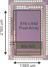
CANOPI -- Analog-to-Information Converter for Compressive Imaging
Applications: Computer Vision, Robotics, Retinal Prosthesis, Smart Infrastructure
Designer: Dr. D. G. Chen
Date: 2012
Analog-to-Information Converters (AIC) take advantage of the limited information bandwidth in
high frequency signals to improve the energy efficiency of front-end data converters in communication
and signal processing systems. Such a scenario is applicable to most image sensors where a high resolution
images typically convey limited information due to the spatial redundancy between neighbouring
pixels. This sensor uses a mixed-signal AIC integrated inside
its SAR ADC to perform real-time image compression during frame capture. The proposed design is fully-dynamic and consumes no
static power. The fabricated prototype consumes 12 pJ per pixel at 111 fps in the image compression
mode and 48 pJ per pixel at 28.7 fps in raw data mode (9b per pixel) under the same clock. To the
best of our knowledge, this is the most energy efficient compressive CMOS image sensor ever reported
in the literature; thanks to the proposed AIC scheme and low-power circuit techniques.
|
|
|
|
| |
|
|
|
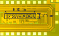
Neural Transceiver based on Micro-Stimulator and SAR ADC
Applications: Biomedical Implants, Retinal Prosthesis
Designer: Dr. D. G. Chen and P. J.-H. Lee
Date: 2012
This chip integrates a micro-stimulator and SAR ADC to demonstrate bilateral neural interface for retinal prosthesis applications.
|
|
|
|
| |
|
|
|
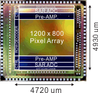
Mega-pixel Color Image Sensor
Applications: Mobile, Security, Webcam
Designer: Dr. F. Tang, Dr. D. G. Chen, and Prof. A. Bermak
Date: 2011
A low-power mega-pixel image sensor with column-parallel 11-bit two-step quantization ADC. It consists of a 3-bit single-slope analog-to-digital converter (ADC) and an 8-bit successive approximation register (SAR) ADC. The power consumption of the column-parallel circuitry is significantly reduced when compared with the traditional single-slope ADC and other low-power ADC schemes because the SAR ADC uses pDAC and smaller reference voltages (reduced by the single-slope MSBs). In addition, as only an 8-bit SAR ADC is required in the proposed quantization scheme, the capacitor array matching can be greatly relaxed compared with an 11-bit SAR ADC thus, resulting in noncalibration feature. The 1200 x 800 pixel resolution color CMOS image sensor (CIS) is fabricated using TSMC 0.18-um CIS technology. The measurement result shows that the total power consumption figure-of-merit of this research is only 1.33 mW/mega-pixel/frame under 3.3-V (analog)/1.8-V (digital) power supply.
|
|
|
|
| |
|
|